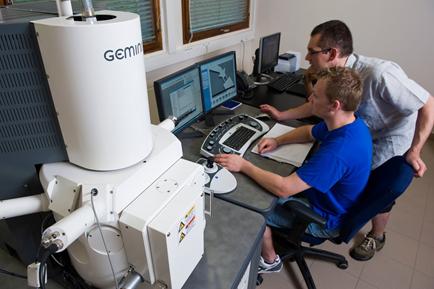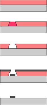


 How can we build and connect nanometric objects? To make electronic circuits based on metal (superconducting or not), we use stencil techniques: materials are patterned thanks to a nanostencil, a resin mask (Plexiglas actually) the edges of which are drawn with a scanning electron microscope.
A computer drives the electron beam that breaks the resin chains according to the pattern drawn thanks to drawing software (type CAD: Computer-aided design). After the resin is developed (it is plunged in a selective solvent that only dissolves the chains broken by the electrons), we get a mask sitting above a substrate. This mask is then put in a vacuum vessel (cf. picture of a deposition chamber with three vacuum vessels), and when the needed metal is heated, atoms can be fired through the holes of the stencil in order to build the metal circuit. After the mask is dissolved, only the circuit remains, deposited above the substrate.
To connect molecules smaller than a nanometre, a little more imagination is required…
Deposition chamber with several vacuum vessels to deposit metals and insulators. Thanks to this chamber, we can make nanometric circuits containing superconducting metals (aluminium, niobium, tantalum), non-superconducting metals (copper, gold, platinum, palladium), and Josephson functions thanks to aluminium oxide.
 The stencil method for nanolithography :
For more details, watch IEF/Minerve video
